
The 74HC595 device has 8bit serial in parallel out shift register that feeds directly to the 8bit D type storage register. The 8bit serial shift register has its own input clock name SH_CP. The D latch 8 bit registers use pin named ST_CP for latching the 8bit shift registers output to D latch output registers.
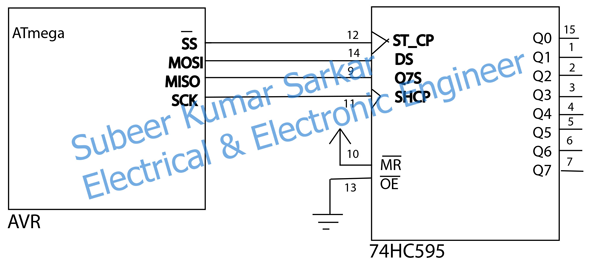
In normal port operation the connection diagram as follow
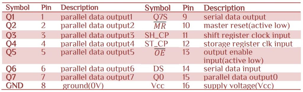
Pin description
Here slave selection bit SS use to trigger the ST_CP (for output latching). Data out through MOSI to DS and data in through Q7S to MISO. Here maximum output frequency 100MHz. Let look at the function available for this chip-
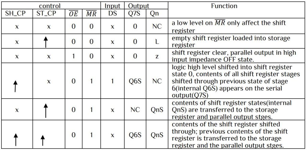
Let interface the chip to AVR. Here AVR works as Master and Shift register works as Slave. One thing notes that the Master generates the clk and slave response to that clk. Since the maximum output frequency is 100MHz for the slave we select Mode0 with double SPI speed. Since from the connection diagram with MR = 1, OE = 0 and the control function it can be seen that we can easily use this shift register with-

Now let’s build a SPI Read/Write function for using this shift register. Since the microcontroller acts as Master so our first step is to initialize AVR as Master with Mode0 double SPI speed. Let’s use ATmega8 for this purpose. SPI initialization function-
#define SPI_DDR 	DDRB
#define SPI_PORT	PORTB
#define SPI_MOSI    DDB3
#define SPI_MISO	DDB6
#define SPI_SCK 	DDB5
#define SPI_SS_DISPLAY   	DDB2
#define SPI_CS_DISPLAY   	PINB2
#define SPI_SS_CONTROL   	DDB1
#define SPI_CS_CONTROL   	PINB1
void init_spi(void)
{
/**** Set MOSI,SS, SCK as output and MISO as input ****/
SPI_DDR =(1<<SPI_MOSI)|(1<<SPI_SCK)|(1<<SPI_SS_CONTROL)|(1<<SPI_SS_DISPLAY);
SPI_DDR&=~(1<<SPI_MISO);
/******************************************************/
SPI_PORT&=~(1<<SPI_CS_DISPLAY);  //enable latch dsplay
SPI_PORT&=~(1<<SPI_CS_CONTROL);  //enable latch control
SPCR|=(1<<SPE)|(1<<MSTR);
SPSR|=(1<<SPI2X);
}
Now let’s make a single Read/Write function. The write procedure consist of following steps

Here 2 shift register is used, one is to control the seven segment display and another one is to display digits.
void SPIWrite_display(unsigned char datain) -> display digits
void SPIWrite_display(unsigned char datain)
{
SPDR=datain;
	while(!(SPSR&(1<<SPIF)))
		{
		;//// Wait for transmission complete
		}
SPI_PORT |= (1<<SPI_CS_DISPLAY);
_delay_us(2); // Hold pulse
// Disable Latch
SPI_PORT &= ~(1<<SPI_CS_DISPLAY);
// Return Serial In Value in MISO
}
void SPIWrite_control(unsigned char datain) -> Control the display
void SPIWrite_control(unsigned char datain)
{
SPDR=datain;
	while(!(SPSR&(1<<SPIF)))
		{
		;//// Wait for transmission complete
		}
SPI_PORT |= (1<<SPI_CS_CONTROL);
_delay_us(2); // Hold pulse
// Disable Latch
SPI_PORT &= ~(1<<SPI_CS_CONTROL);
// Return Serial In Value in MISO
}
We learn how to interface seven segment in I/O section, we also learn how to display digits. Some changes are made to interface in SPI. Let’s look-
void print(unsigned long int num) -> main display part
unsigned long int digits[MAX_DIGIT],i,digit[MAX_DIGIT];
uint8_t control;
void print(unsigned long int num)
{
for(i=0;num!=0;i++)
	{
	digits[i]=num%10;
	digit[i]=seven_segment(digits[i]);
	num=num/10;
	}
	/* main part display number*/
	for(i=0;i<MAX_DIGIT;i++)
	{
	    control=pow(2,MAX_DIGIT)-1;
	    SPIWrite_control(control);
		_delay_ms(1);
		SPIWrite_display(digit[i]);
		control&=~(1<<i);
		SPIWrite_control(control);
		_delay_ms(1);
		control=pow(2,MAX_DIGIT)-1;
		SPIWrite_control(control);
		_delay_ms(1);

	}
}
Here MAX_DIGIT is the maximum number of seven segments we want to control. The main program as follow-
#include<avr/io.h>
#include<util/delay.h>
#include"spi.h"
#include"segment.h"
int main(void)
{
init_spi();
while(1)
	{
	print(3221);
	}
return 0;
}


 Electronic Real Wrold


 Visit Today : 132
 Total Visit : 34309